|

Photovoltaics
The "photovoltaic effect" is the basic physical process through which a PV cell converts sunlight into electricity. Sunlight is composed of photons, or particles of solar energy. These photons contain various amounts of energy corresponding to the different wavelengths of the solar spectrum. When photons strike a PV cell, they may be reflected or absorbed, or they may pass right through. Only the absorbed photons generate electricity. When this happens, the energy of the photon is transferred to an electron in an atom of the cell (which is actually a semiconductor). With its newfound energy, the electron is able to escape from its normal position associated with that atom to become part of the current in an electrical circuit. By leaving this position, the electron causes a "hole" to form. Special electrical properties of the PV cell—a built-in electric field—provide the voltage needed to drive the current through an external load (such as a light bulb).
p-Types, n-Types, and the Electric Field
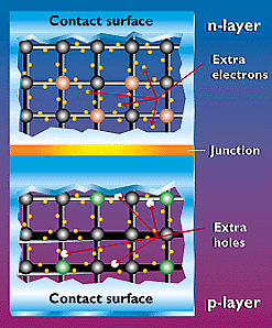 To induce the electric field within a PV cell, two separate semiconductors are sandwiched together. The "p" and "n" types of semiconductors correspond to "positive" and "negative" because of their abundance of holes or electrons (the extra electrons make an "n" type because an electron actually has a negative charge). Although both materials are electrically neutral, n-type silicon has excess electrons and p-type silicon has excess holes. Sandwiching these together creates a p/n junction at their interface, thereby creating an electric field.
When the p-type and n-type semiconductors are sandwiched together, the excess electrons in the n-type material flow to the p-type, and the holes thereby vacated during this process flow to the n-type. (The concept of a hole moving is somewhat like looking at a bubble in a liquid. Although it's the liquid that is actually moving, it's easier to describe the motion of the bubble as it moves in the opposite direction.) Through this electron and hole flow, the two semiconductors act as a battery, creating an electric field at the surface where they meet (known as the "junction"). It's this field that causes the electrons to jump from the semiconductor out toward the surface and make them available for the electrical circuit. At this same time, the holes move in the opposite direction, toward the positive surface, where they await incoming electrons.
Making n and p Material
The most common way of making p-type or n-type silicon material is to add an element that has an extra electron or is lacking an electron. In silicon, we use a process called "doping."
We'll use silicon as an example because crystalline silicon was the semiconductor material used in the earliest successful PV devices, it's still the most widely used PV material, and, although other PV materials and designs exploit the PV effect in slightly different ways, knowing how the effect works in crystalline silicon gives us a basic understanding of how it works in all devices.
Absorption and Conduction
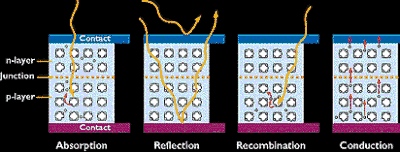 In a PV cell, photons are absorbed in the p layer. It's very important to "tune" this layer to the properties of the incoming photons to absorb as many as possible and thereby free as many electrons as possible. Another challenge is to keep the electrons from meeting up with holes and "recombining" with them before they can escape the cell. To do this, we design the material so that the electrons are freed as close to the junction as possible, so that the electric field can help send them through the "conduction" layer (the n layer) and out into the electric circuit. By maximizing all these characteristics, we improve the conversion efficiency* of the PV cell.
To make an efficient solar cell, we try to maximize absorption, minimize reflection and recombination, and thereby maximize conduction.
*The conversion efficiency of a PV cell is the proportion of sunlight energy that the cell converts to electrical energy. This is very important when discussing PV devices, because improving this efficiency is vital to making PV energy competitive with more traditional sources of energy (e.g., fossil fuels). Naturally, if one efficient solar panel can provide as much energy as two less-efficient panels, then the cost of that energy (not to mention the space required) will be reduced. For comparison, the earliest PV devices converted about 1%-2% of sunlight energy into electric energy. Today's PV devices convert 7%-17% of light energy into electric energy. Of course, the other side of the equation is the money it costs to manufacture the PV devices. This has been improved over the years as well. In fact, today's PV systems produce electricity at a fraction of the cost of early PV systems.
Reprinted from U.S. Department of Energy Photovoltaics Program
Why Silicon & How It Makes a Solar Cell
Silicon has some special chemical properties, especially in its crystalline form. An atom of silicon has 14 electrons, arranged in three different shells. The two shells closest to the nucleous are completely full. The outer shell, however, is only half full (having only four electrons). A silicon atom will always look for ways to fill up its last shell (which would like to have eight electrons). To do this, it will share electrons with four of its neighbor silicon atoms. That's what forms the crystalline structure, and that structure turns out to be critical to PV cells.
Pure silicon is a poor conductor of electricity because none of its electrons are free to move about, locked as they are in the crystalline structure. The silicon in a solar cell is modified slightly so that it will work as a solar cell.
A solar cell has silicon with impurities -- other atoms mixed in with the silicon atoms. We usually think of impurities as being undesirable, but in our case, our cell wouldn't work without them. Consider silicon with an atom of phosphorous here and there, maybe one for every million silicon atoms. Phosphorous has five electrons in its outer shell, not four. It still bonds with its silicon neighbor atoms, but in a sense, the phosphorous has one electron that doesn't have anyone to hold hands with. It doesn't form part of a bond, but there is a positive proton in the phosphorous nucleus holding it in place.
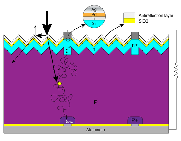
When energy (heat from light) is added to silicon it can force electrons to break free from their atoms. Like kids in a cafeteria, these electrons wander around the crystalline lattice looking for vacant seat. These uncommitted electrons are called free carriers, since they carry an electric current. As mentioned earlier, in pure silicon, all the kids are seated and there are no extra seats. Since there are no kids walking around, it's harder to turn their potential energy into electricity. Our phosphorous doped silicon (doping is the process of adding impurities to silicon) is a different story. The cafeteria is crowded with students (negatively charged electrons) wandering around looking for seats to fill. In fact there are only four chairs for every five students! Hence, it takes a lot less energy to convince one of our "extra" phosphorous electrons to leave the cafeteria. When doped with phosphorous, the resulting silicon is called N-type ("n" for negative) due to the prevalence of all those free electrons wandering around.
|